The USB thumb drive is fast becoming the medium of choice for `pocket' data storage. In this month's project, we will use a very commonly available and inexpensive serial EEPROM device, the Atmel 24C04A, to develop a `toy' thumb drive - toy in the sense our storage device will carry at most 512 bytes (yes, I said `bytes') of data and will be interfaced via the good old parallel port. Our EEPROM device uses the `Inter-IC' (I2C) bus to talk to other devices (the PC or a microcontroller) - we will implement I2C signalling on Linux with two simple device driver programs. To keep the more `application' oriented readers happy, I shall demonstrate how to build a Python `wrapper' over low-level C code and use it to design an elementary GUI in `Tkinter' to access the memory device.
The Inter-IC bus specifies a hardware and software protocol using which multiple Integrated Circuit devices can communicate with each other using just two interconnecting wires. The two wires carry data and a `clock'. The device which generates the clock and initiates/terminates data transfer is called a `master' and the device addressed by the master is a `slave'. Usually, the `master' will be a microcontroller, but in our case, it is a Linux system running a custom program.
EEPROM's are memory devices which can be erased and rewritten electrically. Each byte of memory will have an `address' - a 256 byte device will have cells with addresses from 0 to 255. Data located at a specific address in a serial EEPROM device can be retrieved by transmitting an 8 bit address bit-by-bit (serially); the device will respond by sending out the data in a serial manner.
The EEPROM device which we are using, the 512 byte Atmel 24C04A, supports the I2C protocol.
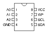
Figure 1 shows the pinout of the device; it comes in a tiny 8 pin package. The pins marked SDA and SCL are the ones which we are interested in - they are the `serial data' and `serial clock' pins respectively. We will connect them to pins on the PC parallel port (remember, the PC is the `master' device). The A0, A1 and A2 pins are used for assigning a `hardwired' address to the device; the Atmel 24C04 device uses only A1 and A2 - we will connect them both to system ground to provide an address of `0'. The `WP' pin is for write protection. If it is connected to the power supply, write operations are disallowed.
The SDA pin is bi-directional; both the master to slave and slave to master communication is via this pin. We will connect parallel port pin 2 (an output pin) as well as pin 10 (an input pin) to the SDA pin of the memory device. This way, the master can send data out to the slave by toggling pin 2 and the data from the slave can be read by looking at the status of pin 10. The SCL pin is connected to output pin 3 of the parallel port.(Note: the SDA pin of the memory device is an `open collector' output - so we don't interface it directly to the parallel port. Instead, we use a simple device, a 7407 `hex open-collector buffer' to do the interface. The circuit schematics, together with ready-to-run source code, is available at http://pramode.net/lfy-mar/)
In some of my earlier articles, we had seen how to do output with the parallel port. Doing input is equally simple; many pins are `input' pins and you can read the logic level on them by simply looking at the bits in a particular `status register'. Listing 1 shows a function which returns 1 or 0 depending on whether the input pin 10 (mapped to bit 6 of the status register) is at a logic HIGH or LOW state.
Figure 2 is a flow chart of the steps involved in writing a byte of data to the memory device.
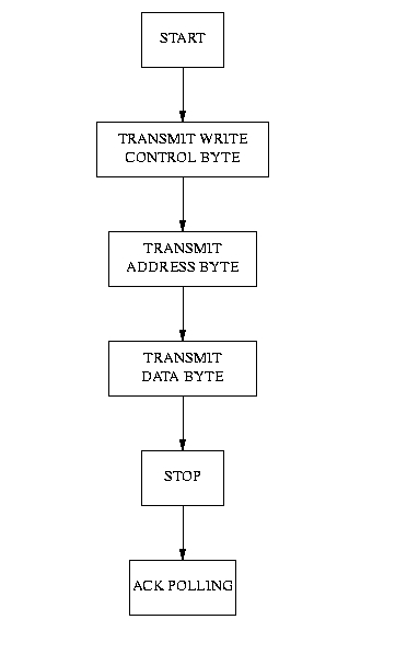
The master device initiates the transaction by sending a START signal. This is followed by a `control' byte which is used for both selecting the device (based on its hardwired address) and indicating whether the transaction will involve a read or a write. Next, the master sends an 8 bit address (the address of the memory cell we wish to write to) followed by the actual data to be written. The master waits for an acknowledgment after transmitting each byte; after the third byte (the data to be written), the master generates a STOP signal. Once the slave gets the STOP, it starts erasing the data at the specified address and replaces it with byte it has obtained from the PC. Let's look at the code which implements each of these steps in detail.
Every I2C bus transaction begins with a START condition and ends with a STOP. START is defined as:
A HIGH to LOW transition on the SDA pin while the
SCL pin is held HIGH.
and STOP is defined as:
A LOW to HIGH transition on the SDA pin while the
SCL pin is held HIGH.
START and STOP are two `special' states in that at all other times, data on the SDA pin will change only when the SCL pin is LOW. Listing 2 shows two functions which implement START and STOP. The functions sda_high, scl_high etc simply drive the parallel port output pins (connected to SDA and SCL) high and low.
Listing 3 defines a function `send_byte' which transmits an 8 bit sequence in MSB first order over the SDA line. In the body of the loop, we extract each bit (starting from the MSB) and depending on whether it is 1 or 0, we drive the SDA line high or low. Note that the clock line is LOW at the time we place the data bit over SDA; the receiver will latch on to the bit during the high period of the clock.
The receiver (EEPROM device) will transmit an acknowledgment (SDA low) when another clock is applied by the master after the 8 data bits are shifted out. The `send_byte' function returns this `acknowledge bit'.
Looking at the flowchart once again, we note that the second step in a `write' transaction is sending a `control byte'. Let's see how to construct this control byte.
When addressing EEPROM devices, the most significant four bits of the byte should set to binary 1010. The next two bits should be the hardwired device address; we have connected pins A2 and A1 of the device to ground, so these two bits should be set to 00. The first six bits are:
1 0 1 0 0 0After sending this byte (using the send_byte function), we will be transmitting the 8 bit address of the location to which data is to be written to. A 512 byte device can be addressed only using 9 bits; this creates a problem. The solution is simple. The next bit of the control word should be a 1 if the address that we transmit is larger than 255, otherwise, it should be a 0. This bit in fact acts as the most significant bit of the address. If we wish to write to say a location whose address is 312, the first seven bits of the control byte would be:
1 0 1 0 0 0 1What remains to be filled up is the last bit. It should be a 0 if we are doing a write and 1 if we are doing a read. So the complete `write control byte', for writing to location 312, becomes:
1 0 1 0 0 0 1 0
Listing 4 is a straightforward translation of the flowchart into C code. We start off by constructing a control byte. The bus transaction begins with a START. First the control byte is written, then the address and then comes the data. The write is assumed to have failed if proper acknowledgment is not received from the slave after each byte is transmitted.
When the STOP condition is transmitted, the slave device starts an internal rewriting operation as a result of which the data byte gets written to the address specified. How do we know that this operation is over? Simple. We just keep on sending a START and a write control byte - the device will not acknowledge until the internal rewriting operation is complete.
The procedure for reading a byte from a random address is a bit peculiar. After a START, we have to send a write control byte and then the required address. We should then discontinue the write operation by transmitting another START condition. A read control byte should then be transmitted. The device will now respond with 8 bits of data which the master has to read by continuously applying clock pulses and sampling the SDA line. If the master sends an acknowledge (by pulling the SDA line low) in the ninth clock period, the slave will respond with the next data byte; if the master doesn't send an acknowledge, the slave will stop sending data. The master has to terminate the transaction with a STOP.
The complete code is available as a small library, i2clib.c, at http://pramode.net/lfy-mar/. It was originally written by Alan Yates; readers would like to to visit http://www.vk2zay.net/eeprom-programmer.html for more information.
Nobody doubts the fact that a Very High Level Language like Python speeds up development considerably. You get higher quality code at a much faster rate. But in situations were you wish to interact directly with the hardware, C is still the best choice. So is the case when you are writing highly timing sensitive code or code which has to run blazing fast.
But what if only a part of your code is doing low level manipulations? You get the best of both worlds by writing that part in C, and the major portion in Python! Let's explore this idea a bit more in detail.
Making C functions callable from Python is easier than you think, provided you use a wonderful tool called SWIG (available from http://www.swig.org). Let's look at how we can make three functions from our `i2clib.c' library Python callable. Two of these functions are `read_data' and `write_data' while the other one, `enable_io', simply calls the `iopl' function to gain access to the I/O ports.
We will first create a header file containing declarations of all the functions which we need to access from Python (let's call it `i2clib.h'):
int read_data(int address);
int write_data(int address, unsigned char data);
void enable_io(void);
We will now execute the command:
swig -python -module i2c -o i2c_wrap.c i2clib.hThe result will be two files, `i2c.py' and `i2c_wrap.c'. We will compile i2c_wrap.c and i2clib.c to object files and link them to generate a library called `_i2c.so':
cc -c -I/usr/local/include/python2.3/ i2c_wrap.c
cc -c i2clib.c
ld -shared i2clib.o i2c_wrap.o -o _i2c.so
We can now interactively verify that we are able to communicate with the EEPROM device. Here is a sample interaction at the Python prompt (the code should be executed as superuser after connecting the EEPROM device to the parallel port and powering it up):
>>> from i2c import *
>>> enable_io()
>>> write_data(10, 123)
>>> read_data(10)
123
>>> a = [read_data(addr) for addr in range(512)]
>>>
Isn't it great to be able to use cute Python tricks like list comprehension on our hardware device?
Driver code which performs only very elementary device access using in/out instructions need not be written as part of the OS kernel; as such, our serial EEPROM driver needs to exist simply as a user space program. Only when we start playing around with things like interrupts do we need to seriously think about building a kernel-space driver. But newbie Linux kernel programmer's shouldn't miss out the chance of writing a kernel module to control a simple (but non-trivial) hardware device like our serial EEPROM memory; it's a great learning experience!
Listing 5 is a fragment of code taken from a `toy' driver I wrote for accessing the memory device. The only function of interest is the `ioctl'. We define two ioctl requests, RANDOM_READ_BYTE and RANDOM_WRITE_BYTE. The byte read request accepts a user-space pointer to integer (in `ioctl_param'). Upon entry, the integer pointed to by this argument will contain the address of a byte to be read; upon return, it will be changed to the actual value of the byte. The byte write request accepts as argument a user space pointer to structure (of type `address_data'); the structure contains two fields which store the address of the EEPROM cell to be written to, and the value to write. Once the module is compiled and loaded into the kernel and a device file with an appropriate major number is created (the major number allotted to our driver can be found out by examining /proc/devices), we can execute the test program shown in Listing 6.
The Python interpreter provides a reasonably good interface to major Linux system calls.Listing 7 does exactly the same thing as the C test program in Listing 6. To understand the logic of the code, you need to know how the `pack' and `ioctl' functions work.
The `struct' module is very useful when doing low level I/O. An invocation of the form:
struct.pack('II', 1, 2)
will result in the interpreter returning a string
of the form:
'\x01\x00\x00\x00\x02\x00\x00\x00'You will observe that the first four elements of this string are the individual bytes of the number 1 expressed in little endian format and the next four elements, those of the number 2. A C structure containing two integers will be mapped to exactly this form in memory (note that the first argument to `pack' is a `typecode', the two upper case I's signify the fact that exactly two other arguments follow and they should be interpreted as unsigned integers).
The Python ioctl function works this way: if it's last argument is an immutable buffer, then a copy of the buffer is passed to the operating system and the return value is a string of the same length containing whatever the operating system put into it. If the kernel ioctl method returns -EIO, it is reported as an exception by the interpreter.
In one of my earlier articles, I had presented FLTK as being an ideal C/C++ GUI toolkit for the hardware hacker. In the Python world, there is an equally amazing (but sometimes underestimated) toolkit called Tkinter. Let's wind up our project by building a small GUI to test access to the EEPROM device.
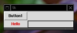
Listing 8 is a short and sweet Python-Tkinter program; if you get a feel of how this works, you pretty much understand most of Tkinter. Figure 3 is the output generated by the program.
Every Tkinter program should have a `root widget' which is an ordinary window. The statement:
root = Tk()creates this widget and stores a reference in the variable `root'. All the other widgets are `children' of the root widget. First we create a button and assign an event handler; you press the button and the function `fun' will get executed. Next, the button has to be given a place in the root window - this is done by invoking the `grid' function. We visualize the root window as being a 2-by-2 matrix; the button will be placed in the very first cell (row=0 and column=0). Next we create a Label widget (which is just a text message) and an Entry widget (which can be used for entering as well as displaying text) and assign them certain positions within the grid.
With this much of background, an absolute beginner to Tkinter programming should be able to craft Listing 9 on her own in under 10 minutes flat; that's the beauty of this toolkit! Figure 4 is the output generated by the program.
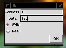
The code makes use of two radio buttons, an ordinary button and two text entry fields. Whenever the button is clicked, the function `button_callback' is invoked. It reads the value in the first text entry box (the address) and then checks which radio button is pressed, `read' or `write'. Each radio button in a group has associated with it a unique `value'; all buttons in the same group also maintain a reference to a shared object (in our program, the object V of type IntVar). Whenever a radio button is activated, the value associated with it is assigned to the shared object; thus it is possible for us to know just be extracting the integer value stored in this object which radio button is active. Depending on this, we invoke either the `read_data' or `write_data' function (C functions made available to Python via SWIG).
There are several directions in which the project can be extended. At the hardware level, you can try using higher capacity devices like the 24C08, 24C16 etc. You might also think of chaining multiple 24C04 devices together. Designing a USB interface would be much harder, but is well worth the effort.
The device manual describes read/write modes other than the single byte random address read/write which we have implemented. You can try coding them on your own. The graphical user interface can be made more sophisticated. If you want something more challenging, here is another idea. In one of my earlier articles, I had described how to go about writing file system code in user space using a package called FUSE. You can use FUSE to implement a simple filesystem on the memory device; you can now use the memory chip like a USB thumb drive! Be a bit imaginative, and invent more projects on your own!
Authoritative information regarding the I2C bus is available at http://www.semiconductors.philips.com/markets/mms/protocols/i2c
Python/Tkinter programming is examined in detail at http://www.pythonware.com/library/tkinter/introduction. The Python source distribution comes with a good number of demo programs; reading them is the best way to learn this toolkit.
Readers interested in SWIG can read an old Linux Gazette article at http://linuxgazette.com/issue49/pramode.html.
The February issue of LinuxFocus (http://linuxfocus.org) has an article on I2C and Linux written by Guido Socher.