gEDA PCB
Published on: 2007-11-26
gEDA PCB
2007-11-26T18:28:58
Got a set of PCB's (designed using gEDA tools) today - this is my second attempt at using gEDA tools (after the AVR Badge experiment).
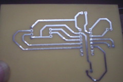
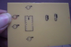 The board will carry a MAX232 to perform TTL<->RS232 level shifting.
The design files will be made available soon ...
Lots of students are starting blogs these days - check out this one by a third sem CS fellow.
The board will carry a MAX232 to perform TTL<->RS232 level shifting.
The design files will be made available soon ...
Lots of students are starting blogs these days - check out this one by a third sem CS fellow.
Gopu
Tue Nov 27 15:47:08 2007
It is very nice to see students blogging about their experiments, reminds me of my own electronics days for the four (short lived) engineering years! Gopu.